Table of Contents
Report Description
The market for thin wafer processing and dicing equipment has been covered under the scope of this report. The market is expected to witness strong growth during the forecast period. This is mainly due to thin wafer processing and dicing equipment manufacturers are continuously focusing on expanding their production units across different parts of the globe, which in turn is anticipated to be a major driving factor for the global thin wafer processing and dicing equipment market.

Rapidly growing demand for portable communication and electronic devices such as smart phones, memory cards, smart cards, and other computing devices across the globe is expected to augment the demand for the fabrication of miniature integrated circuit packages. Manufacturing of wafer-level packaging and 3D integration usually requires a significant reduction in wafer thickness. An increasing number of applications take advantage of this reduced size of wafer thickness. This, in turn, is anticipated to boost the demand for thin wafer processing and dicing equipment at an exponential rate in the coming years.

The importance of processing and dicing thin wafers is increasing for a variety of different products and applications. The product road maps of many devices point towards increasing usage of thinner and ultra-thin dies. Therefore, this creates a better opportunity for various thin wafer processing and dicing equipment during the forecast period from 2017 to 2025. In terms of both value (USD Million) and volume (units), the global market is expected to grow at an exponential rate in the coming years.
Thin Wafer Processing and Dicing Equipment Market Segments
The global thin wafer processing and dicing equipment market has been segmented on the basis of:
- Application
- Wafer thickness
- Dicing technology, and
- Region
It also provides a cross-sectional analysis of the market across different regional segments such as Asia-Pacific, Europe, North America, Asia-Pacific (APAC), Middle-East & Africa (MEA), and South America under its scope. Attributes such as better electrical performance, improved form factor due to thin packaging, and reduced cost of manufacturing a device obtained by using a thin wafer is the primary factor responsible for the growing demand for thin and ultrathin wafers during the forecast period from 2017 to 2025.
Scope of the Report
A complete analysis of market dynamics, which includes the market drivers, restraints, and opportunities, is included within the scope of the report. The market dynamics for the different segments, namely applications, wafer thickness, and dicing technology, have been covered separately under the purview of the report. Additionally, the country-level trend for each region has also been covered under the scope of the report. Thus, this report provides an exhaustive study of the global thin wafer processing and dicing equipment market and also provides a forecast of the market for the period from 2017 to 2025.
Market Dynamics
Increasing demand for smaller die and thinned wafer across various application sectors especially from the smart phone and smart card industry is the primary factor anticipated to foster the demand of the market during the forecast period from 2016 to 2024. Thinned wafers are also increasingly used across various MEMS (Microelectromechanical Systems), memory and, logic devices and power devices among others as it offers reduced form factors along with better high heat dissipation and improved electrical performance. In addition, the current trend of miniaturization of devices having superior performance and lower cost of configuration is also anticipated to boost the demand of thinned wafers even below 100 µm and 50 µm. This factors, in turn is expected to drive the demand of technologically advanced thin wafer processing and dicing equipment in order to achieve desired miniaturization of semiconductor devices.

High-level Analysis Covered In the Report
Under the scope of the report on global thin wafer processing and dicing equipment market, several high-level analyses have been covered. This includes:
- The product-market trend analysis
- Product life-cycle analysis
- Porter’s five forces analysis, and
- Market attractiveness analysis
Key trends analysis discusses the current and upcoming trends in this market. Product life-cycle analysis analyses the current life-cycle stage of the product in the five wide geographic regions, such as whether the product is approaching maturity in a region or whether it is a new entrant, etc. Porter’s five forces analysis provides insights into the competitive scenario with regards to new entrants, substitutes, buyers, and suppliers. To provide a detailed insight into the global thin wafer processing and dicing equipment market, attractiveness analysis has been provided in the report. The market attractiveness analysis details the investment attractiveness by application, wafer thickness, dicing technology, and geography.
The Competitive Profiling
The competitive profiling of the key players in the global thin wafer processing and dicing equipment market and their business segments has been exhaustively covered under the purview of the study. Moreover, key business strategies adopted by the leading players in the market have also been covered under the scope of the report.
Key Competitors in the Thin Wafer Processing and Dicing Equipment Market
The leading operating in the thin wafer processing and dicing equipment industry included:
- EV Group (Austria)
- Lam Research Corp (The U.S), Plasma-Therm LLC (The U.S)
- DISCO Corp.(Japan), Tokyo Electron Ltd.(Japan), Tokyo Seimitsu Co. Ltd.(Japan), and Panasonic Corp.(Japan)
- Advanced Dicing Technologies (Israel)
- Suzhou Delphi Laser Co. Ltd.(China)
- SPTS Technologies Ltd. (U.K) among others.
Report Highlights
- Impeccable insights related to relevant segment of the market.
- In depth analysis of key trends of the market.
- In-depth analysis of the competitive landscape and competitor behavior in the market.
- Major push factors that will affect the growth of the market.
- Growth possibilities in different segments of the market till 2025.
- Key strategies implemented by the market leaders to sustain growth in the market.
- Major restraining factor of the market.
- Ways to generate new revenue streams.
Segmentation Overview
Application Segment
In addition, different application segments including logic and memory, MEMs (Microelectromechanical Systems), power devices, RFID (Radio Frequency Identification) and CMOS (Complementary Metal Oxide Semiconductor) image sensors in which thin wafer processing and dicing equipments are majorly utilized has also been included within this scope of research. Moreover, depending on dicing technology, the market has been categorized into blade dicing equipment, laser dicing equipment and plasma dicing equipment. Each of the application segment and dicing technology has been further classified into wafer thickness in order to highlight which wafer size is majorly used in which application segments.
- Logic and Memory
- Micro Electro Mechanical Systems (MEMS)
- Power Device
- Radio Frequency Identification (RFID)
- CMOS Image Sensor
Thickness of Wafer
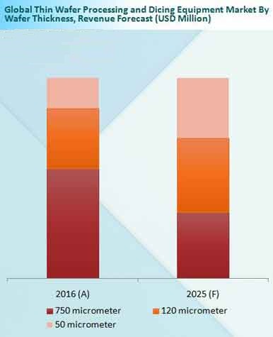
Based on thickness of wafer, the thin wafer processing and dicing equipment market has been classified into 750 μm, 120 μm and 50 μm. Among the different thickness of wafer, though the 750 μm segment held the largest market share in 2016, the 750 μm of wafer thickness is expected to lose its dominance and is increasingly replaced by the 120 μm of wafer thickness owing to its increasing adoption across various RFID and power devices coupled with initiatives taken by various automotive manufacturers as a part of their social responsibility to reduce CO2 gas emission from automotives by interchanging the mechanical part with portable power electronic system in order to increase electrification in the cars.
- 750 Micrometer
- 120 Micrometer
- 50 Micrometer
Dicing Technology
Among the different dicing technology, the laser dicing technology is anticipated to witness the highest growth during the forecast period for 2017 to 2025. Laser dicing technology does not require any water and thus it offers the most suitable choice for dicing wafers required for various sensors. Moreover, Laser dicing is also used abundantly in combination with blade dicing for various applications.
- Blade Dicing
- Laser Dicing
- Plasma Dicing
Thin Wafer Processing and Dicing Equipment Market: By Geography
- North America (U.S. and Canada)
- Europe (U.K., Germany, France, CIS + Scandinavia and Rest of Europe)
- Asia-Pacific (China, Japan, India, South Korea and Rest of Asia-Pacific)
- Middle East & Africa (Israel, South Africa and Rest of Middle East & Africa)
- South America (Brazil, Mexico and Rest of South America)
Regional Outlook

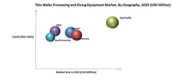
Geographically, the Asia-Pacific region overshadowed the other regions’ markets both in terms of revenue generation and growth and is expected to maintain its leading position through the forecast period. The wide concentration of various thin wafer processing and dicing equipment manufacturers in this region, coupled with rapid investments and innovation activities taking place in this region in order to develop advanced equipment and overcome the limitations of the existing equipment, is the primary factor attributed to this region’s high market share and growth.


